
【转】HFCBGA封装
HFCBGA封装
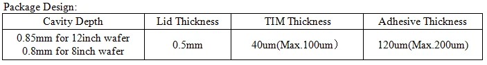

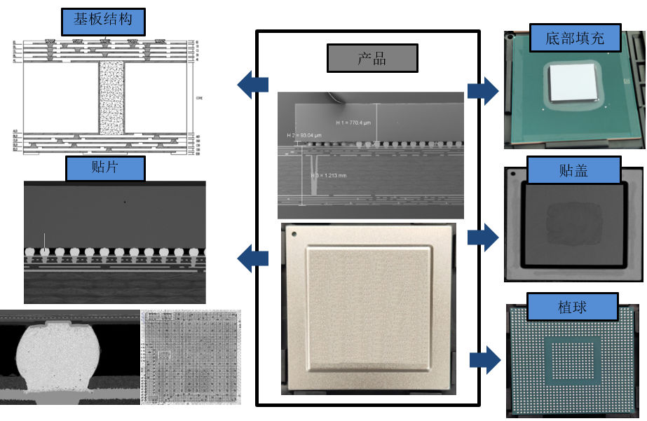
HFCBGA主要产品结构
封装尺寸(mm)
芯片面积
(mm²)
Bump
数量
Ball size
(mm)
基板
层数
基板厚度(mm)
27x27
75+
2000+
0.6
8层
0.76
35x35
170+
4500+
0.6
10层
1.25
37.5x37.5
250+
6000+
0.6
12层
1.35
40x40
180+
5000+
0.6
12层
1.33
40x40
260+
7000+
0.6
12层
1.33
HFCBGA项目案例
FCBGA
适用于各种终端应用的灵活性设计
主页
|
封装
|
层压板
|
FCBGA
查看相关下载内容
改善电气性能与 IC 功能
Amkor 的倒装芯片 BGA (FCBGA) 封装采用先进的单器件层压板或陶瓷基板。FCBGA 基板利用多个高密度布线层,激光盲孔、埋孔和叠孔,超小节距金属化,从而实现最高的布线密度。通过将倒装芯片互连与超先进基板技术结合在一起,FCBGA 封装能够在最大程度上优化电气性能。在确定电气性能以后,倒装芯片所带来的设计灵活性也将增加最终封装设计的选项。Amkor 为众多产品格式提供 FCBGA 封装,以满足各种终端应用需求。
技术解决方案
基板
4-18 层积层基板
高 CTE 陶瓷
无核
凸块类型
共晶锡/铅
无铅(绿色)
铜柱凸块(阵列和小节距外围)
封装格式
裸晶
有盖
Abstract
Document Sections
Authors
Figures
References
Citations
Keywords
Metrics
Footnotes
-
Introduction
-
Materials and Experiment Details
-
Result and Discussion
-
Conclusions
High Power Large Size HFCBGA Thermal Characterization
Publisher: IEEE
PDF
CP Hung
All Authors
(Show More)
Introduction
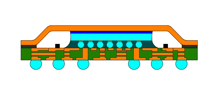
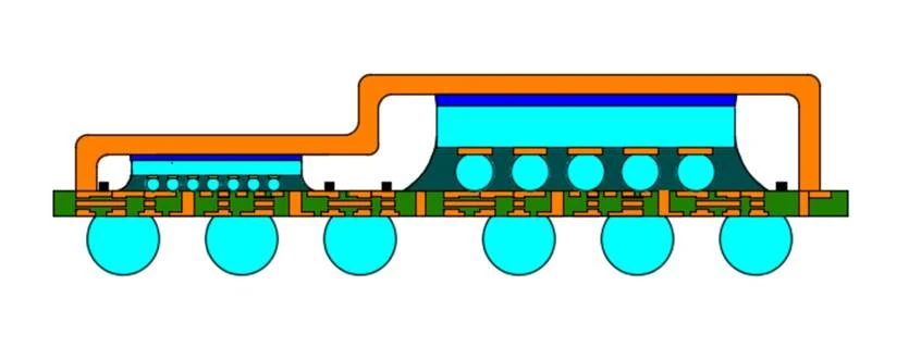
Accompany the growth of integrated infrastructure for big data and intelligence analytics, the requirement of high power large size integrated circuit (IC) package for data center plays a crucial role. Flip chip ball grid array (FCBGA) is the mainstream of this kind of application, no matter integrates the functions by system on a chip (SoC), multi chips module (MCM), fan-out (FO) or 2.5D. FCBGA has a substrate with chips flipped on it; high performance FCBGA (HFCBGA) is a subset of FCBGA, which specifies the FCBGA has a heat slug attached on the substrate include the types of stiffener ring only, one-piece cavity type, one-piece hat type, two-piece type (thermal lid + stiffener ring) and thermal lid only (DLA, direct lid attach). For high power application, e.g., hundred watts power dissipation, a heat sink on the top of the package for heat dissipation is the universal method for thermal design. At this situation, chip exposed design packages, include FCBGA and stiffener ring only HFCBGA, have the best thermal performance, due to minimize the thermal resistance between chips and heat sink. However, it makes chips loss the protection from lid and exposure to damage risk under any uncertain forces. Therefore, HFCBGA with a lid for chip protection becomes a popular choice.
Sign in to Continue Reading
特色
最大为 31 毫米的晶粒尺寸
从 10 毫米至 67.5 毫米的封装尺寸(正在开发 85 毫米)
0.4 毫米、0.5 毫米、0.65 毫米、0.8 毫米和 1.0 毫米节距 BGA
90 µm 最小阵列凸块节距
<90 µm 最小外围凸块节距
其他封装选项
晶圆节点 ≥7 nm 已合规,正在为 5 nm 申请合规资质
顶部和底部 SMT 元件
多晶粒模块
存储器元件合封在顶部
多种可选的盖板材料
接地盖板
BGA尺寸可定制
